Control of Preferred Orientation of Pt Film
![]()
Platinum has been widely used as a bottom electrode in the fabrication of nonvolatile ferroelectric memory because of its chemical stability and catalytic effect of enhancing oxygen diffusion from the oxygen support layer to the ferroelectric film in order to suppress fatigue properties [37, 38]. In order to obtain the highest polarization from the PZT film, a highly (100)-oriented Pt film should be deposited so that a (001) PZT film can easily be grown on it, similar to epitaxial growth, owing to a seed layer of the (100) Pt film. However, the production of highly (100)-oriented Pt film is generally difficult, since the Pt(111) plane has the lowest surface energy because it has the greatest density of lattice points for the face-center cubic structure, a (111)-oriented Pt film is generally grown preferentially on substrates. Only a few researchers have so far succeeded in preparing highly (100)-oriented Pt films. Most of them used single-crystal oxide substrates to obtain epitaxial (100) Pt films. For example, Ahn and Baik [39] observed a drastic change in the preferential orientation once the epitaxial Pt film was grown on a (100) MgO single-crystal substrate by sputtering. At high substrate temperatures and low deposition rates, epitaxial (100) Pt films are grown preferentially. This result is explained by the competing roles of the film surface and the film/substrate interfacial energies during the nucleation stage. Recently, Akai et al. [40] have successfully prepared an epitaxial (100) Pt film on a (100) Si substrate using an epitaxial g-Al2O3 (100) buffer layer, and Okamoto et al. [41] have produced an epitaxial Pt film with a preferential (100) orientation on a Y2O3-stabilized ZrO2 (YSZ) film on a (100) Si substrate, using an epitaxial (100) Ir buffer layer by sputtering. They convincingly explained their results by considering the lattice mismatch between the film layers. However, from the viewpoint of industrial mass production, because single-crystal substrates are very expensive, epitaxial Pt films are not useful. On the other hand, Kim et al. [42] reported that a Pt film with a (100) preferential orientation on an SiO2/Si substrate could be obtained by adding O2 gas to the Ar sputtering gas and adjusting the ratio between O2 and Ar flow rates during sputtering. They showed that the change in the preferential orientation of the Pt film results from the Pt lattice distortion induced by oxygen incorporation. However, in this method, the substrate temperature must be more than 400oC, which is unfavorable for mass production. Therefore, in order to obtain (100)-oriented Pt films at a lower substrate temperature, a new deposition technique is required.
To satisfy this requirement, the crystallographic orientation of polycrystalline Pt films on RuOx/SiO2/Si substrates was investigated without epitaxial growth or oxygen during sputtering, using various conditions of sputtering power, sputtering gas pressure and deposition time. It will be shown that the preferential orientation, (100) or (111) of the Pt film can be controlled by adjusting the sputtering power, pressure and film thickness. Then, the formation mechanism of the preferential (100) orientation of the Pt film will be discussed with respect to competition between the surface energy and the strain energy due to intrinsic stress in the Pt film.
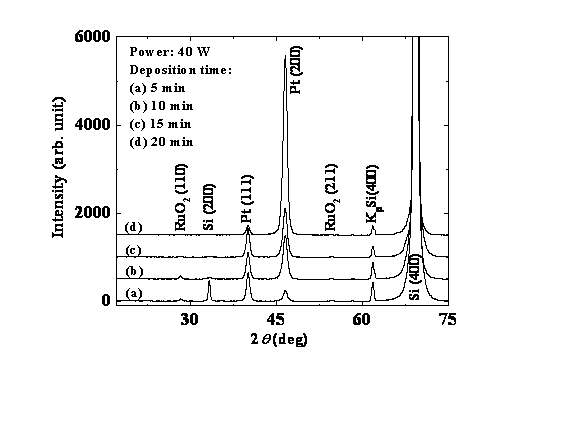
3.1 Pt Film Thickness as a Function of Deposition Time
 Figure
3.1 shows the dependence of the Pt film thickness on the deposition time for
sputtering powers of 10 to 60 W at a sputtering gas pressure of 10 Pa. It is
clear that the film thickness increases linearly with deposition time, which
means that the deposition rate any power is constant. Also, the deposition rate
of the slope increases with sputtering power because a higher power induces a
higher sputtering rate. Hence, following this result, the thickness can be
controlled by adjusting the deposition time and sputtering power.
Figure
3.1 shows the dependence of the Pt film thickness on the deposition time for
sputtering powers of 10 to 60 W at a sputtering gas pressure of 10 Pa. It is
clear that the film thickness increases linearly with deposition time, which
means that the deposition rate any power is constant. Also, the deposition rate
of the slope increases with sputtering power because a higher power induces a
higher sputtering rate. Hence, following this result, the thickness can be
controlled by adjusting the deposition time and sputtering power.
3.2 Effect of Sputtering Power and Deposition Time on Pt Film Orientation
 Figure
3.2 shows typical 2q-q
XRD patterns of the Pt films deposited on RuOx/SiO2/Si
substrates for 10 min at 10 Pa, where Figs. 3.2(a)-(c) are for the sputtering
powers of 20, 30 and 40 W, respectively. In all of the measured XRD patterns, it
can be observed that only two main peaks of (111) and (200) for Pt. Thus,
hereafter, the Pt(200) and Pt(111) peaks are focused and discussed. Although the
intensity of the Pt(111) peak seems to be almost the same for any sputtering
power, the intensity of the Pt(200) peak drastically increases when the
sputtering power increases from 20 to 30 W. However, the Pt(200) peak decreases
slightly when the power increases to 40 W. From this result, it can be
considered that the volume of the (111) Pt crystalline region hardly or slightly
depends on the power or thickness because the thickness increases with power for
a constant deposition time as shown in Fig. 3.1. On the other hand, the volume
of the (100) Pt crystalline region strongly depends on the power or thickness.
Figure
3.2 shows typical 2q-q
XRD patterns of the Pt films deposited on RuOx/SiO2/Si
substrates for 10 min at 10 Pa, where Figs. 3.2(a)-(c) are for the sputtering
powers of 20, 30 and 40 W, respectively. In all of the measured XRD patterns, it
can be observed that only two main peaks of (111) and (200) for Pt. Thus,
hereafter, the Pt(200) and Pt(111) peaks are focused and discussed. Although the
intensity of the Pt(111) peak seems to be almost the same for any sputtering
power, the intensity of the Pt(200) peak drastically increases when the
sputtering power increases from 20 to 30 W. However, the Pt(200) peak decreases
slightly when the power increases to 40 W. From this result, it can be
considered that the volume of the (111) Pt crystalline region hardly or slightly
depends on the power or thickness because the thickness increases with power for
a constant deposition time as shown in Fig. 3.1. On the other hand, the volume
of the (100) Pt crystalline region strongly depends on the power or thickness.
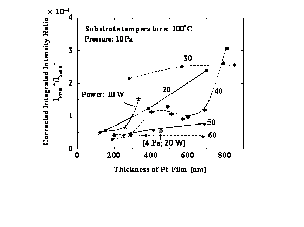
Figure 3.3 shows typical 2q-q XRD patterns of Pt films deposited at 40 W and 10 Pa, where Figs. 3.3(a)-(d) are for the deposition times of 5, 10, 15 and 20 min, respectively. For the Pt(111) peaks, their features are similar to the above results shown in Fig. 3.2, i.e., they have almost same intensities for any deposition time except 20 min. However, the intensity of the Pt(200) peak increases with deposition time or thickness because of the constant power of 40 W, which means that the volume of the (100) Pt crystalline region has a strong positive correlation with the thickness. However, taking the results shown in Fig. 3.2 into account, the increase in the thickness due to increasing the power does not always enhance the (100) Pt crystalline growth. From the results shown in Figs. 3.2 and 3.3, the dependence of the Pt film orientation on the thickness seems somewhat complicated. Thus, in order to clarify this dependence, the volume ratios of the (100) and (111) Pt crystalline regions over the total volume of the Pt film is estimated, using the corrected integrated intensities IPt200* and IPt111* for Pt(200) and Pt(111), respectively.
3.3 Dependence of Corrected Integrated Intensities on Pt Film Thickness
In order to evaluate the volume ratios of the Pt(100) and Pt(111) regions over the whole deposited Pt film, the integrated intensity Ihkl from the (hkl) plane in the measured XRD pattern is used. The Ihkl was corrected by the film thickness because the penetration depth of the X-ray for Pt, ~ 2 mm, [43] is greater than the film thickness, < 900 nm, in this study. Also, Ihkl was normalized by the integrated intensity of Si(400) in order to compensate for fluctuation of the X-ray beam intensity on the diffracted intensity. Here, the corrected integrated intensity is denoted as Ihkl*. The details of the correction and normalization are given in Appendix G.
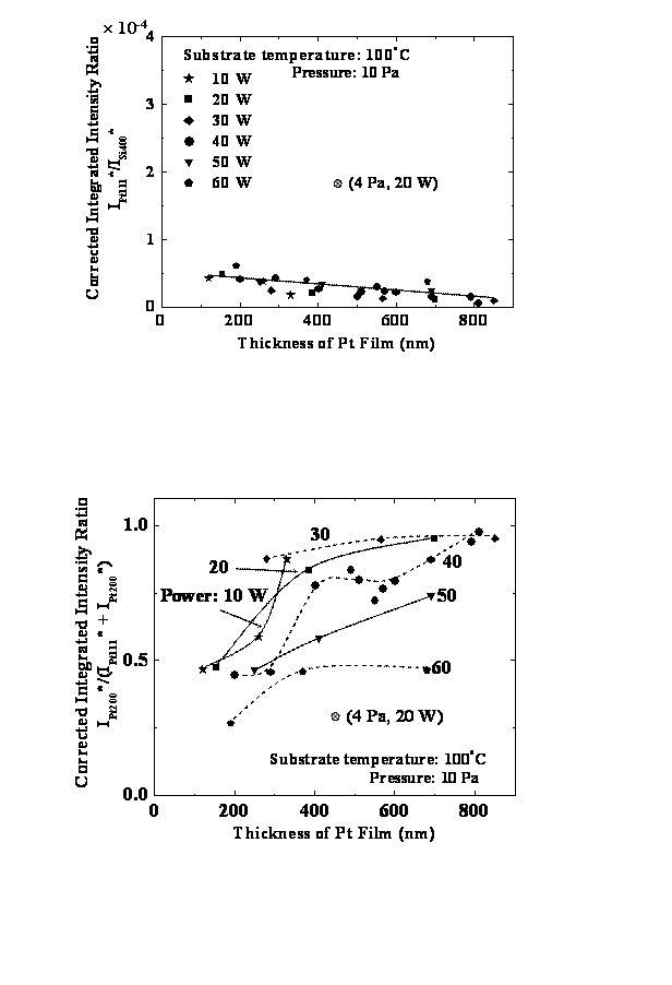
Figure 3.4 shows the corrected integrated intensity ratio IPt200*/ISi400* as a function of Pt film thickness for the sputtering powers from 10 to 60 W at 10 Pa, where the datum for 4 Pa, Ä, is mentioned in § 3.4. Here, it should be noted that this ratio is an index corresponding to the volume ratio of the (100) Pt crystalline region, not its absolute volume ratio because the measured integrated intensity was normalized not by a perfectly crystallized Pt film but by the Si substrate. From this figure it can be seen that, on the whole, IPt200*/ISi400* increases with the thickness of the Pt film for any power, which means that the volume ratio of the (100) oriented region in the Pt film increases with film thickness. Also, IPt200*/ISi400* strongly depends on sputtering power. That is, the ratio for the lower power < 30 W is high and that for the higher power > 50 W is low. However, the behavior for 40 W is different and seems to be a transition from the lower power to the higher power, which is further discussed later. Figure 3.5 shows the corrected integrated intensity ratio IPt111*/ISi400*, an index corresponding to the volume ratio of the (111) Pt crystalline region as a function of Pt film thickness. It is obvious that the (111)-oriented crystalline volume ratio slightly decreases with thickness irrespective of sputtering power, and that the ratio is much less than (100)-oriented ratio for films thicker than 400 nm. This means that the (111)-oriented region is hardly grown with increasing thickness in contrast to the (100)-oriented region. In order to compare the volume ratio between the (100) Pt crystalline region and the (111) Pt crystalline region directly, the integrated intensity ratio of IPt200*/(IPt111* + IPt200*) as a function of Pt film thickness for the various sputtering powers of 10 to 60 W at 10 Pa is plotted as shown in Fig. 3.6. The maximum ratio of 1 and the minimum ratio of 0 indicate that the (100) orientation and the (111) orientation, respectively, are perfectly predominant. From Fig. 3.6, it can be seen that for the thinner films of 100 to 200 nm, the integrated ratio, or the volume fraction of the (100) orientation, is almost equal to that of the (111) orientation except for the highest power of 60 W. Also, on the whole, the volume fraction of the (100) orientation increases with thickness. Furthermore, increasing sputtering power suppresses the increase in ratio, i.e., the growth of the Pt(100)-oriented crystalline region, in particular, for 60 W. Here, it should take a notice of the next point. The vertical axis of Fig. 3.6 does not indicate crystalline volume fraction over the whole film but volume fraction between the (100) region and the (111) region. That is, a higher ratio in Fig. 3.6 does not always mean a larger volume fraction of the (100) crystalline region in the Pt film. For example, at 20 W, although the ratios at around 400 and 700 nm are almost the same and about 0.8, the volume ratios of Pt (100) in Fig. 3.4 are very different from each other. This means that the whole film is not crystalline and some regions might be in the amorphous phase. Also, XRD can hardly detect some oriented planes owning to the extinction rule even if the region is perfectly crystallized. Next, the mechanism of this volume fraction behavior to film thickness and power will be discussed.
3.4 Discussion on Growth Mechanism of Pt Film
The most common explanation of the preferential orientation of the deposited film is based on the crystallographic plane with the lowest surface energy, e.g., 1.66 J m-2 for Pt (111) [44]. However, the above experimental results can not be understood by this mechanism. This is because the preferential orientation of the Pt film changes with thickness to the (100) plane whose surface energy is not the lowest, 2.17 J m-2 [44]. Thus, it is necessary to consider another driving force that governs the preferential orientation. Some researchers have suggested that the driving force is to minimize the overall energy of the film, U0, which is composed of not only surface energy but also strain energy [45]. While surface energy is constant, irrespective of film thickness, strain energy is directly proportional to thickness, assuming that stress is uniform throughout the film. That is, if surface energy is predominant, the film grows toward the crystallographic plane with the lowest surface energy. If strain energy is predominant, the film grows toward the plane with the lowest strain energy. Next, the discussion focuses on strain energy in the film.
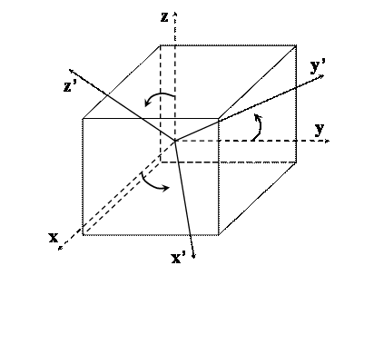
All crystalline materials are elastically anisotropic even with cubic symmetry such as Pt. This anisotropy gives rise to an orientation dependence of the elastic strain energy of the crystalline film when it is placed in a nonhydrostatic stress field. In this result, the stress field is a biaxial one approximately parallel to the surface of the film. The internal stress existing in the film is composed of intrinsic stress and thermal stress. Thermal stress is generated during cooling after deposition, but the cause of intrinsic stress is more complicated. It has been reported that in the sputtered film, intrinsic stress depends on the flux and energy of particles striking the film [46]. McKenzie et al. have reported the theoretical calculation of the orientation dependence of elastic strain energy in cubic crystals [47]. At constant temperature and stress level s with a biaxial stress field applied in the x’-y’ plane, as shown in Fig. 3.7 for a cubic crystal, the Gibbs free energy G per unit volume is
![]() (3.1)
(3.1)
![]() , (3.2)
, (3.2)
where G0 is the
orientation–independent and standard Gibbs free energy, sij
are the components of the 6
´
6 compliance matrix, the
si’
are the diagonal components of the 1
´
6 stress tensor ![]() , which is obtained from the standard uniaxial stress tensor
, which is obtained from the standard uniaxial stress tensor
![]() by rotational transformation from the standard x-y-z
system to the x’-y’-z’ system in three dimensions, as shown in Fig. 3.7.
According to their theory, G for biaxial stress in the x’-y’ plane
is expressed in terms of uniaxial stress
by rotational transformation from the standard x-y-z
system to the x’-y’-z’ system in three dimensions, as shown in Fig. 3.7.
According to their theory, G for biaxial stress in the x’-y’ plane
is expressed in terms of uniaxial stress
![]() which indicates the crystallographic orientation of the film
surface. That is, the
which indicates the crystallographic orientation of the film
surface. That is, the ![]() is not actual stress but a provisional stress for
convenience. C has a minimum value of zero when the
is not actual stress but a provisional stress for
convenience. C has a minimum value of zero when the
![]() is aligned in the [100] direction, and C has a maximum
of 1/3 when
is aligned in the [100] direction, and C has a maximum
of 1/3 when ![]() is aligned in the [111] direction. If the value of
is aligned in the [111] direction. If the value of
![]() (3.3)
(3.3)
is less than zero, G is minimized when C
= 1/3 or the provisional stress ![]() is aligned in the [111] direction. In this case, the
orientation of the film surface is [111]. On the other hand, if
d
is positive, G will be minimized when C = 0 or
is aligned in the [111] direction. In this case, the
orientation of the film surface is [111]. On the other hand, if
d
is positive, G will be minimized when C = 0 or
![]() is aligned in the [100] direction. In this case, the
orientation is (100), and the orientation-dependent strain energy is zero.
For Pt, the values
of s11, s12 and s44 are
listed in Table 3.1 [48]. Using these values, it can be calculated that
d
= 0.387 > 0. This means that a (100)-oriented Pt film has a minimum strain
energy per unit volume independent of its thickness.
is aligned in the [100] direction. In this case, the
orientation is (100), and the orientation-dependent strain energy is zero.
For Pt, the values
of s11, s12 and s44 are
listed in Table 3.1 [48]. Using these values, it can be calculated that
d
= 0.387 > 0. This means that a (100)-oriented Pt film has a minimum strain
energy per unit volume independent of its thickness.
Table 3.1 Components of elastic compliance tensor for Pt [48].
Also, for film case, strain energy is mainly due to intrinsic stress generated during deposition but not thermal stress. This is because the temperature difference during deposition is so small, about 77oC, that it can not generate a large thermal stress to make the orientation change. In fact, thermal stress sth was estimated using the following integral formula with respect to temperature T:
 ,
(3.4)
,
(3.4)
where YPt = 170 GPa and nPt = 0.39 are the Young’s modulus and Poisson ratio of Pt, respectively. Td and Tr are the deposition temperature and room temperature, respectively. Also, aPt = 9 ´ 10-6 deg-1 and aSi = 2.5 ´ 10-6 deg-1 [49, 50] are the thermal expansion coefficients of Pt and Si, respectively. Using eq. (3.4), thermal stress is calculated to be 139 MPa. This value is much smaller than the reported value of a few GPa which includes both thermal stress and intrinsic stress in Pt film [49, 50]. Also, some researchers have reported that stress in molybdenum [51] and tungsten [52] films can be changed from tensile to compressive by increasing the sputtering power, which is accomplished principally by increasing the current and deposition rate. If the sputtering power is low, the density of sputtered particles is small because sputtering cathode power is the product of plasma current and plasma voltage. In this case, the Pt film contains considerably more porous microstructures and impurities leading to intrinsic tensile stress. However, if the sputtering power is high, the density of sputtered particles is high. The Pt film exhibits a denser microstructure of sputtered particles, i.e., it contains a smaller amount of porous microstructures and impurities, which reduces tensile intrinsic stress and leads to compressive intrinsic stress, compared with the case of low power. As mentioned above, the film stress for low power is toward the tensile stress and for high power is toward compressive.
Figure 3.8 shows schematic diagrams for the variation of the U0 of the Pt film with the film thickness t for the Pt(111) and Pt(100) planes, where Figs. 3.8 (a) and 3.8 (b) indicate the low-power case and high-power case, respectively. The energies at zero thickness represent the surface energies S100 and S111 for Pt(100) and Pt(111) planes, respectively, and strain energies are proportional to film thickness, where strain energy consists of orientation-dependent and -independent components, and stress is assumed to be uniform throughout the film. Although the actual stress s is not constant but a function of thickness, it is supposed that this model is valid for qualitatively understanding the physical phenomena occurring in the film. Since the strain energy of the Pt(100) plane is minimum as mentioned before, it can be considered that it has only the orientation-independent component. First, the low-power case of Fig. 3.8 (a) is discussed, where tcr is the critical thickness at which U0 for the Pt(111) plane is equal to that for the Pt(100) plane. Since the contribution of surface energy to the difference in U0 is predominant below tcr, U0 for the (111) plane is lower than that for the (100) plane. On the other hand, the contribution of strain energy becomes predominant above tcr, and U0 for the (100) plane is lower. That is, owning to the driving force needed to minimize the overall energy of the film, the (111) orientation is developed below tcr, whereas the (100) orientation is developed above tcr. Since the (111)- and (100)-oriented volume ratios for the films thinner than 200 nm are almost equal as shown in Fig. 3.6, tcr can be estimated to be less than 100 nm, and the predominant orientations of the lower layer below tcr and the upper layer over tcr are (111) and (100), respectively.


This growth situation is shown schematically in Fig. 3.9, which depicts the film growth model for the low- and high-power cases. According to this model, U0 for the (100) Pt film and the (111) Pt film are expressed approximately by
 (3.5)
(3.5)
![]() , (3.6)
, (3.6)
respectively, where A is the area of the film, and s0 and sn0 are orientation-dependent stress and orientation-independent stress, respectively. At t = tcr, U0(100) = U0(111), and hypothesizing s0 » sn0, we can obtain tcr approximately as
![]() .
(3.7)
.
(3.7)
By substituting a reasonable value of 2 GPa into s0 as in some reports [49, 50], tcr is calculated to be approximately 30 nm. This value is acceptable in these experimental results shown in Fig. 3.6. For the thickness > 300 nm, since the film beyond tcr has mainly a (100)-oriented crystalline phase, the volume of the Pt(100) orientation region is much larger than that of the Pt(111) orientation region. On the other hand, for high power ³ 50 W, as shown in Fig. 3.9 (a), the (111)-oriented crystalline phase is generated near the interface similar to the low-power case, because the driving force of the (111) phase is the lower surface energy of S111 and is almost independent of power. As mentioned before, increasing sputtering power reduces tensile stress; thus, total stress is decreased under these experimental conditions. Therefore, strain energy density is not so large for tcr to be much larger, as shown in Fig. 3.8 (b). Also, increasing sputtering power induces serious damage in the crystal structure of the deposited film because it enhances the flux and energy of the particles bombarding to the film. Probably, the effects of both larger tcr and heavier bombardment of particles at high powers result in the growth of the (100)-oriented crystalline phase being suppressed, as shown in Fig. 3.9 (b). For the power of 40 W, the behavior of the orientation in terms of the thickness is different from that for other powers, and 40W seems to be a transitional power. This is because this intermediate power suppresses tensile stress neither strongly nor weakly, and gives some damage to the film more or less.
Furthermore, in order to verify this model, we deposited the Pt film at a sputtering gas pressure of 4 Pa instead of 10 Pa and a low power of 20 W. Lowering the gas pressure from 10 Pa increases the film density because the amount of sputtering Ar gas as an impurity in the film is decreased; thus, film stress may be reduced. As a result, for the 450-nm-thick Pt film, lower integrated intensity ratios of IPt200*/ISi400* = 0.6 ´ 10-4 is obtained as shown in Fig. 3.4, higher IPt111*/ISi400* = 1.8 ´ 10-4 as shown in Fig. 3.5, and lower IPt200*/(IPt111* + IPt200*) = 0.28 as shown in Fig. 3.6, than those at 10 Pa, which means that (111) crystalline growth is enhanced and its volume ratio becomes much larger upon decreasing the gas pressure from 10 to 4 Pa. Therefore, it can be said that this model depicts the essential physical phenomena in the deposited film and that it is valid experimentally in spite of insufficient strictness.
3.5 Summary
The summary of this chapter is as follows:
1. The preferential orientation of Pt films deposited on the RuOx/SiO2/Si substrates at a substrate temperature of 100oC by RF magnetron sputtering using only Ar gas without O2 gas was investigated. It was found that the volume ratio of the (100)-oriented region over the whole film increases with film thickness for various sputtering powers of 10 to 60 W. Also, the ratio for low power £ 30 W is higher than that for high power ³ 50 W, and approximately decreases with power. On the other hand, the volume ratio of the (111)-oriented region is smaller and slightly decreases with film thickness irrespective of sputtering power.
2. These results can be explained by surface energy and strain energy. Strain energy, mainly due to intrinsic stress, increases with thickness, while surface energy is independent of thickness. Also, increasing sputtering power reduces intrinsic tensile stress owning to the denser film and induces crystalline damage in the deposited film. Generally, it can be considered that if the contribution of surface energy to the difference in overall energy U0 is predominant, the preferential orientation tends toward Pt(111), but if that of strain energy is predominant, the preferential orientation tends toward Pt(100). Therefore, for thinner film, since the surface energy of the Pt(111) orientation is the lowest, the Pt (111)-oriented crystalline phase is easily grown. Also, for a thicker film and lower power, since strain energy increases owning to tensile stress and U0(111) is larger than U0(100), the (100)-oriented crystalline phase is mainly grown.
3. However, even for thicker film, when strain energy or tensile stress is reduced by the density increase in the deposited film due to increased power or lowered gas pressure, the (111)-oriented crystalline phase becomes dominant in the deposited film. In accordance with this result, we can control the preferential orientation of the Pt film by adjusting the sputtering power, pressure and deposition time which influence the thickness, intrinsic stress and crystallization of the deposited film.